

- Description
- Product Enquiry
Overview:
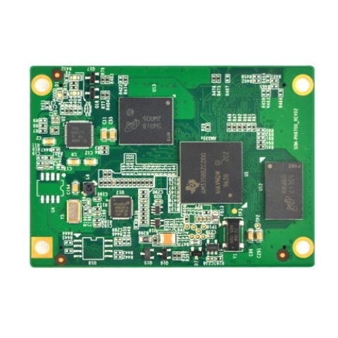
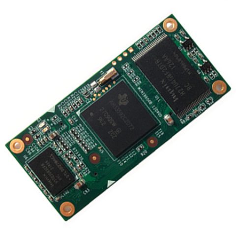
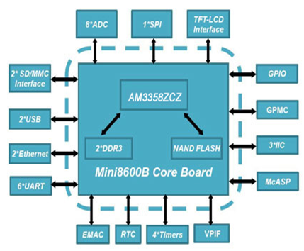
Measuring 60mm by 27mm, a controller board based on TI’s Sitara AM3358 ARM Cortex-A8 high performance processor. The tiny module integrates 2*256MBytes DDR3 SDRAM and 512Mbytes NAND Flash, and uses two 0.4mm space 2*40-pin board-toboard male expansion connectors.
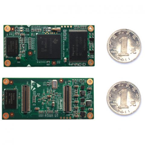
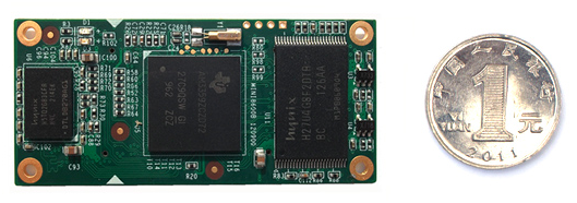
Top-view of SOM-AM335x-MM (Part NO: Mini8600B) CPU Module

Bottom-view of SOM-AM335x-MM (Part NO: Mini8600B) CPU Module


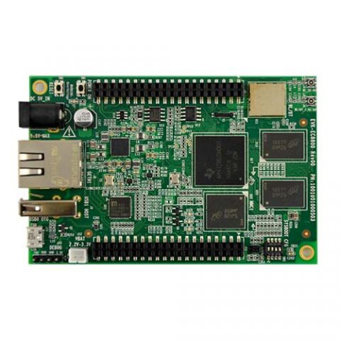
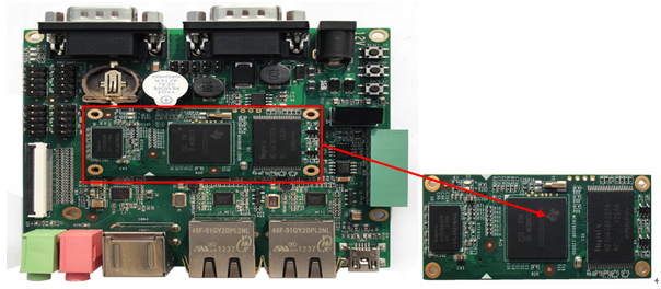
Embest has designed a single board computer SOM-AM335x-MM with standard baseboard (Part NO: SBC8600B) which has an expansion board to carry the SOM-AM335x-MM (Part NO: Mini8600B). The flexible design allows the fast and easy way of realizing and upgrading the controller’s capabilities. In additional to those features offered by SOM-AM335x-MM (Part NO: Mini8600B), the SOM-AM335x-MM with standard baseboard (Part NO: SBC8600B)features 5 serial ports (including 2 RS232 and 3 TTL), 2 USB Host and 1 USB OTG, 2 Ethernet ports, CAN, RS485, LCD, Touch screen, Audio, ADC and more other peripherals. The SBC8600B is a ready-to-run platform to support for Linux 3.2.0, Android 4.0 and WinCE 7 operating systems.(No support WinCE for industrial version).
SOM-AM335x-MM with standard baseboard (Part NO: SBC8600B)

System block diagram:

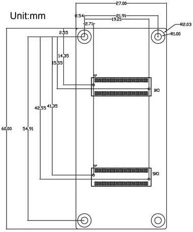
Dimension:

Hardware Features:
Processor/Memory:
-
TI AM3358 ARM Cortex-A8 microprocessor
– 1GHz ARM Cortex-A8 32-bit RISC MPU
– NEON™ SIMD Coprocessor
– 32KB/32KB of L1 Instruction/Data Cache with Single-Error Detection (parity)
– 256KB of L2 Cache with Error Correcting Code (ECC)
– SGX530 Graphics Engine
– Programmable Real-Time Unit Subsystem
-
2*256MByte DDR3 SDRAM
-
512MByte NAND Flash
Expansion Interfaces and Signals Routed to Pins:
-
Two 0.4mm space 2*40-pin board-to-board male expansion connectors
-
TFT LCD Interface (support 24-bpp parallel RGB Interface LCD)
-
2 * USB 2.0 OTG Ports With Integrated PHY, High-Speed
-
3 * inter-integrated circuit (I2C) Bus interfaces
-
6 * UART interfaces;
-
1 * SPI interface;
-
Two 10/100/1000 Mb/s Ethernet MAC (EMAC) with Management Data Input/Output
-
(MDIO) module;
-
A multichannel audio serial ports (McASP);
-
8-channel 12-bit ADC interfaces;
-
Two 4-line SD/MMC card interfaces;
-
GPMC bus
Electrical Features:
-
Dimensions: 60.0 mm x 27.0 mm
-
PCB Layers: 8 layers
-
Temperature: 0~70 Celsius ( commerial )
-40 ~ 85 Celsius(industrial)
-
Humidity Range: 20% ~ 90%
-
Input Voltage: 3.3V
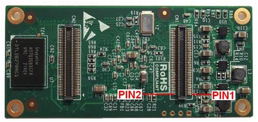
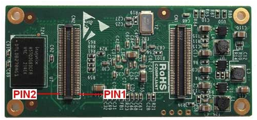
Embest SOM-AM335x-MM (Part NO: Mini8600B) CPU Module is connected to the carrier board via two 0.4mm space 2*40-pin board-to-board male expansion connectors.
The connector marked in red below is CN1; table 1-1 described the pin signals of CN1 connector.

|
CN1 |
||
|
Pin |
Signal |
Description |
|
1 |
GND |
GND |
|
2 |
VDDS_RTC |
Supply voltage for RTC |
|
3 |
CLK_OUT1 |
Clock out1 |
|
4 |
CLK_OUT2 |
Clock out2 |
|
5 |
MMC0_DAT0 |
MMC0 data bus |
|
6 |
MMC0_DAT1 |
MMC0 data bus |
|
7 |
MMC0_DAT2 |
MMC0 data bus |
|
8 |
GLOBLE_RESETN |
SYS_RESET IN/ OUTPUT |
|
9 |
MMC0_DAT3 |
MMC0 data bus |
|
10 |
AM335X_PWRON_RESETN |
CPU PWRON Reset |
|
11 |
GND |
GND |
|
12 |
GND |
GND |
|
13 |
AM355X_PRU_UART0_CTS |
PRU UART0 Clear To Send |
|
14 |
AM355X_PRU_UART0_RX |
PRU UART0 receive data |
|
15 |
AM355X_PRU_UART0_RTS |
PRU UART0 request to send |
|
16 |
AM355X_PRU_UART0_TX |
PRU UART0 transmit data |
|
17 |
AM355X_UART0_RX |
UART0 receive data |
|
18 |
AM355X_UART3_RX |
UART3 receive data |
|
19 |
AM355X_UART0_TX |
UART0 transmit data |
|
20 |
AM355X_UART3_TX |
UART3 transmit data |
|
21 |
AM355X_CAN0_RX |
CAN0 receive data |
|
22 |
AM355X_I2C0_SDA |
I2C0 master serial data |
|
23 |
AM355X_CAN0_TX |
CAN0 transmit data |
|
24 |
AM355X_I2C0_SCL |
I2C0 master serial clock |
|
25 |
AM355X_UART4_RX |
UART4 receive data |
|
26 |
AM355X_UART1_RX |
UART1 receive data |
|
27 |
AM355X_UART4_TX |
UART4 transmit data |
|
28 |
AM355X_UART1_TX |
UART1 transmit data |
|
29 |
GND |
GND |
|
30 |
GND |
GND |
|
31 |
MII1_COL |
MII1 collision detect |
|
32 |
AM355X_USB0_DRVVBUS |
USB0 controller VBUS control output |
|
33 |
MII1_TX_CLK |
MII1 transmit clock |
|
34 |
AM355X_USB1_DRVVBUS |
USB1 controller VBUS control output |
|
35 |
MII1_TX_EN |
MII1 transmit enable |
|
36 |
MII1_REF_CLK |
MII1 reference clock |
|
37 |
MII1_TXD3 |
MII1 transmit data |
|
38 |
MII1_CRS |
MII1 carrier sense |
|
39 |
MII1_TXD2 |
MII1 transmit data |
|
40 |
MII1_RX_ER |
MII1 receive data error |
|
41 |
MII1_TXD1 |
MII1 transmit data |
|
42 |
MII1_RX_DV |
MII1 receive data valid |
|
43 |
MII1_TXD0 |
MII1 transmit data |
|
44 |
MII1_RX_CLK |
MII1 receive clock |
|
45 |
MII_MDIO |
MII MDIO DATA |
|
46 |
MII1_RXD3 |
MII1 receive data |
|
47 |
MII_MDC |
MII MDIO CLK |
|
48 |
MII1_RXD2 |
MII1 receive data |
|
49 |
GND |
GND |
|
50 |
MII1_RXD1 |
MII1 receive data |
|
51 |
AM355X_USB0_DM |
USB0 DM- |
|
52 |
MII1_RXD0 |
MII1 receive data |
|
53 |
AM355X_USB0_DP |
USB0 DP |
|
54 |
MMC0_CMD |
MMC0 Command Signal |
|
55 |
GND |
GND |
|
56 |
USB0_VBUS |
USB0 bus voltage |
|
57 |
AM355X_USB1_DM |
USB1 data- |
|
58 |
AM355X_USB1_ID |
USB1 ID |
|
59 |
AM355X_USB1_DP |
USB1 data+ |
|
60 |
AM355X_USB0_ID |
USB0 ID |
|
61 |
GND |
GND |
|
62 |
USB1_VBUS |
USB1 bus voltage |
|
63 |
GPMC_A0 |
GPMC address |
|
64 |
GPMC_A7 |
GPMC address |
|
65 |
GPMC_A5 |
GPMC address |
|
66 |
GPMC_A11 |
GPMC address |
|
67 |
GPMC_A4 |
GPMC address |
|
68 |
GPMC_A10 |
GPMC address |
|
69 |
GPMC_A3 |
GPMC address |
|
70 |
GPMC_A9 |
GPMC address |
|
71 |
GPMC_A2 |
GPMC address |
|
72 |
GPMC_A8 |
GPMC address |
|
73 |
GPMC_A6 |
GPMC address |
|
74 |
GPMC_A1 |
GPMC address |
|
75 |
GND |
GND |
|
76 |
GND |
GND |
|
77 |
VDD_3V3 |
Power |
|
78 |
VDD_3V3 |
Power |
|
79 |
VDD_3V3 |
Power |
|
80 |
VDD_3V3 |
Power |
The connector marked in red below is CN2; table 1-2 described the pin signals of CN2 connector.

|
CN2 |
||
|
Pin |
Signal |
Description |
|
1 |
GND |
GND |
|
2 |
GND |
GND |
|
3 |
MCASP0_AHCLKX |
MCASP0 transmit master clock |
|
4 |
MCASP0_ACLKX |
MCASP0 transmit bit clock |
|
5 |
MCASP0_FSX |
MCASP0 transmit frame sync |
|
6 |
MCASP0_AXR0 |
MCASP0 serial data(I/O) |
|
7 |
MCASP0_AHCLKR |
MCASP0 receiver master clock |
|
8 |
MMC0_CLK |
MMC0 clock |
|
9 |
MCASP0_FSR |
MCASP0 receive frame sync |
|
10 |
MCASP0_AXR1 |
MCASP0 serial data(I/O) |
|
11 |
GND |
GND |
|
12 |
GND |
GND |
|
13 |
VDDA_ADC |
Supply voltage range for ADC |
|
14 |
AM355X_ADC0 |
ADC0 |
|
15 |
AM355X_ADC1 |
ADC1 |
|
16 |
AM355X_ADC2 |
ADC2 |
|
17 |
AM355X_ADC3 |
ADC3 |
|
18 |
AM355X_ADC4 |
ADC4 |
|
19 |
AM355X_ADC5 |
ADC5 |
|
20 |
AM355X_ADC6 |
ADC6 |
|
21 |
AM355X_ADC7 |
ADC7 |
|
22 |
GND_ADC |
GND ADC |
|
23 |
GND |
GND |
|
24 |
GND |
GND |
|
25 |
LCD_DATA1 |
LCD data bus |
|
26 |
LCD_DATA12 |
LCD data bus |
|
27 |
LCD_DATA0 |
LCD data bus |
|
28 |
LCD_DATA10 |
LCD data bus |
|
29 |
LCD_DATA5 |
LCD data bus |
|
30 |
LCD_DATA13 |
LCD data bus |
|
31 |
LCD_DATA4 |
LCD data bus |
|
32 |
LCD_DATA11 |
LCD data bus |
|
33 |
LCD_DATA6 |
LCD data bus |
|
34 |
LCD_DATA14 |
LCD data bus |
|
35 |
LCD_DATA8 |
LCD data bus |
|
36 |
LCD_VSYNC |
LCD vertical sync |
|
37 |
GND |
GND |
|
38 |
GND |
GND |
|
39 |
LCD_DATA9 |
LCD data bus |
|
40 |
LCD_PCLK |
LCD pixel clock |
|
41 |
LCD_DATA15 |
LCD data bus |
|
42 |
GPMC_AD11 |
GPMC address & data |
|
43 |
LCD_DATA3 |
LCD data bus |
|
44 |
GPMC_AD15 |
GPMC address & data |
|
45 |
LCD_DATA2 |
LCD data bus |
|
46 |
GPMC_AD14 |
GPMC address & data |
|
47 |
LCD_DATA7 |
LCD data bus |
|
48 |
GPMC_WAIT0 |
GPMC wait0 |
|
49 |
LCD_HSYNC |
LCD horizontal sync |
|
50 |
GPMC_BEN1 |
GPMC byte enable 1 |
|
51 |
GND |
GND |
|
52 |
GND |
GND |
|
53 |
LCD_EN |
LCD AC bias enable chip select |
|
54 |
GPMC_WPN |
GPMC write protect |
|
55 |
GPMC_AD13 |
GPMC address & data |
|
56 |
GPMC_CSN3 |
GPMC chip select |
|
57 |
GPMC_AD9 |
GPMC address & data |
|
58 |
GPMC_CSN2 |
GPMC chip select |
|
59 |
GPMC_AD10 |
GPMC address & data |
|
60 |
GPMC_CLK |
GPMC clock |
|
61 |
GPMC_AD8 |
GPMC address & data |
|
62 |
GPMC_AD6 |
GPMC address & data |
|
63 |
GPMC_AD12 |
GPMC address & data |
|
64 |
GND |
GND |
|
65 |
GND |
GND |
|
66 |
GPMC_CSN1 |
GPMC chip select1 |
|
67 |
GPMC_ADVN_ALE |
GPMC address valid/address latch enable |
|
68 |
GPMC_AD5 |
GPMC address & data |
|
69 |
GPMC_BEN0_CLE |
GPMC byte enable 0/Command latch enable |
|
70 |
GPMC_AD4 |
GPMC address & data |
|
71 |
GPMC_OEN_REN |
GPMC output /read enable |
|
72 |
GPMC_AD1 |
GPMC address & data |
|
73 |
GPMC_AD2 |
GPMC address & data |
|
74 |
GPMC_AD0 |
GPMC address & data |
|
75 |
GPMC_AD3 |
GPMC address & data |
|
76 |
GPMC_CSN0 |
GPMC chip select0 |
|
77 |
GPMC_AD7 |
GPMC address & data |
|
78 |
GPMC_WEN |
GPMC write enable |
|
79 |
GND |
GND |
|
80 |
GND |
GND |
Software Features:
|
OS |
Item |
Remark |
||
|
Linux |
BIOS |
SPL |
NAND |
|
|
MMC/SD |
||||
|
FAT |
||||
|
U-boot |
NAND |
|||
|
MMC/SD |
||||
|
FAT |
||||
|
NET |
||||
|
Kernel |
Linux-3.2.0 |
Supports ROM/CRAM/EXT2/EXT3/FAT/NFS/ JFFS2/UBIFS file systems |
||
|
Driver |
NAND Flash, SDRAM, Serial port, RTC, Ethernet, TFT LCD, Touch screen, TF card, USB OTG, Audio input/output, LED, Key, CAN, RS485, Power Management (backlight, PWM, ADC) |
|||
|
2D/3D (not provided with source code) |
||||
|
Android |
Kernel |
Linux-3.2.0 |
Gingerbread |
|
|
Driver |
NAND Flash, SDRAM, Serial port, RTC, Ethernet, TFT LCD, Touch screen, TF card, USB OTG, Audio input/output, LED, Key, Power Management (backlight, PWM) |
|||
|
2D/3D (not provided with source code) |
||||
|
WinCE7 |
BIOS |
X-loader |
NAND |
|
|
MMC/SD |
||||
|
FAT |
||||
|
EBOOT |
NAND |
|||
|
MMC/SD |
||||
|
FAT |
||||
|
NET |
||||
|
OAL |
OAL module |
Boot parameter |
||
|
KILT(EMAC) |
||||
|
Serial debug |
||||
|
REBOOT |
||||
|
Watchdog |
||||
|
RTC |
||||
|
Kernel profiler |
||||
|
System timer |
||||
|
Interrupt controller |
||||
|
MMU |
||||
|
Driver |
NAND Flash, SDRAM, Serial port, RTC, Ethernet, TFT LCD, Touch screen, TF card, USB OTG, Audio input/output, LED, Key, RS485, Power Management (backlight) |
|||
|
CAN, 2D/3D (not provided with source code) |
||||
Applications:
-
Intelligent Display Terminal
-
Medical Equipment
-
Smart Appliances
-
Alternative Energy Device
-
Intelligent Display Terminal
-
Blood analyzer
-
Robotic Arm
-
Charging Station